Core Technologies
TE Connectivity offers global sensor manufacturing services for your design needs including clean room production, rapid prototyping to small serial up to mass production on fully automated production lines.
Capabilities
The Sensor Manufacturing Services (SMS) team at TE Connectivity can provide the expertise with materials and interconnections excellence for full, turnkey solutions from small series to several million pieces. We provide design-to-manufacture, design-to-assembly, feasibility studies, design verification and protyping. Our facilities are certified to ISO 9001, ISO 13485, IATF 16949, ISO 9100, and ISO 14001 standards.
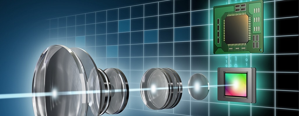
Imager Packaging
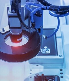
- Large imagers in a cleanroom up to ISO5. Deep material process knowledge that is optimized for extremely low particle count, 2-5µm position accuracy and low warpage with less than 35µm flatness.
- Large arrays are yield optimized high fill-factor tiles with matrix arrays of CT/MRT/PET applications. Experience with flip chip, TSV, radiation hardness, and non-magnetic materials.
- Automated processes for miniature optoelectronic assemblies that are augmented by manual capabilities where necessary.
Development Team
- Board-level and module simulation
- Mechanical simulation (warpage, flatness, distortion)
- Thermal simulation
- Design and materials
- Electric layout, design optimization
- Mechanic design optimization
- Extensive material and process knowledge
- Testing and qualification
- Environmental
- Final test development
Core Technologies

Singulation

Die Bonding

Wire Bonding

Frame Attach / Glob Top / Hermetic Encapsulation

Calibration & Testing
Application Expertise
Industrial
Components and Applications
- Line scan imaging: custom high end machine vision camera board
- Area scan imaging: custom packaging of small to large image sensors
- Time of Flight (ToF) imaging: custom packaging of industrial ToF camera board
Medical
Components and Applications
Digital imaging:
- PET-sensor array
- Endoscopic image sensor
Image signal processing: line driver ASIC assembly flat panel x-ray
Transportation
Components and Applications
- Pressure sensors
- Torque/steering sensors
- Avalanche photodiodes / matrix arrays