Medical Technologies

Microfluidic Chips: 5 Tips to Smooth Your Transition from Prototype to Scale
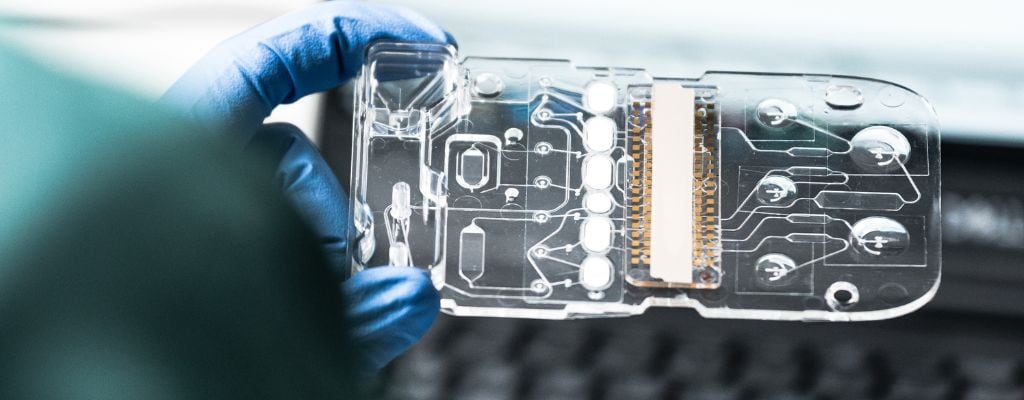
Congratulations! You and your design team have just developed an exciting application that can utilize microfluidics as a device platform. Such a platform can have market potential by virtue of being highly reproducible, lower cost and easy to use. The next phase of commercialization considers finalizing the design for scalable manufacturing e.g., moulding, functionalization, assembling, quality, and other processes involving ramp-up and scale production. Design decisions that seemed appropriate at the prototype phase may have a ‘downstream’ impact on costs and reproducibility and may require reengineering.
The TE Connectivity IVD Solutions team has extensive experience collaborating with customers in designing microfluidic cartridges and self-contained “Lab on a Chip” technologies for life sciences applications that move from prototype to pre-clinical to clinical and ultimately full commercialization. Here are Five Tips from our Microfluidic Design, Clinical Regulatory and Manufacturing teams for consideration to make a smooth transition from “Lab to Launch”.
TE TIP #1
Approach Design as if You are Producing a Million Units Tomorrow
In the approximate 3 to 5 years, it takes to develop and commercialize a microfluidic cartridge and instrument, significant attention may be paid to the timing, money and resources with an emphasis on hitting program milestones quickly while sometimes leaving unresolved issues - rationalizing with comments such as:
1. “Our engineers are smart – we’ll ‘tweak’ the design later”.
2. “We are in the prototype phase and will focus on that issue later.”
However, to transition from 50 prototypes to 500 preclinical samples to 50,000 commercially available devices, creating a strong, yet flexible, plan may be the most direct activity for success, saving time and money.
Some experienced companies apply the Design for Manufacturing and Assembly (DFMA) methodology to mitigate risk at the earliest stages of design and surprises later. For example, applying DFMA may aid in designing a product that can be molded and assembled using commercially available automation equipment. DFMA methodology can also be important when integrating multiple technologies and incorporating input from teams comprising fluid dynamics engineers, electrical engineers, biologists, mold makers,manufacturing assembly specialists and more.
TE TIP #2
While Polydimethylsiloxane (PDMS) can be an Acceptable Prototyping Material, You May Quickly Outgrow It
PDMS can be an excellent material choice for initial prototyping and allows for iterative changes through the prototyping process. It is biocompatible, easy to form and optically transparent. However, it has limitations for moving to a high volume scale and may not be a long-term manufacturing solution.
It is recommended that the selection of a prospective material at the initial design stage considers cost, reproducibility, performance, channel design, assembly, surface properties, moldability, gas permeability and reagent integration. Adjusting to a new material from PDMS can have a significant impact on design and processing.
Certain commonly used materials for microfluidic consumables are summarized in the table below and the suitable choice can be identified using DFMA.
Commonly used Materials and Properties for Microfluidic Chips:
| Gas Permeable |
Water Contact Angle | Chemical Resistance |
Optical Transmission |
Average Tg (°C) |
Chip Fabrication |
Cost at Scale |
|
PDMS Polydimethylsiloxane
|
Yes | 107° | +/- |
90% | 125° | Casting | $$$ |
| PMMA Polymethylmethacrylate | No | 68° | +/- | 92% | 95° | Injection Molding | $ |
PC Polycarbonate |
No | 30° | +/- | 88% | 145° | Injection Molding |
$ |
PS Polystyrene |
No | 94° | +/- | 90% | 100° | Injection Molding | $ |
COP Cyclic Olefin Polymer |
No | 90° | + | 92% | 140° | Injection Molding | $$ |
| COC Cyclic Olefin Copolymer |
No | 90° | + | 92% | 120° | Injection Molding | $$ |
| Silicon | No | 88° | + | 50% | 147° | Machining | $ |
Glass Borosilicate |
No | <15° | + | 95% | 260° | Machining | $$$ |
TE TIP #3
Choose the Optimal Size and Geometry of Microchannels and Features
Selecting a suitable design for the microfluidic circuit can be key to a smooth transition to molding and to assembly. For the preferred performance of the fluidic elements, time may be well spent planning out the “plumbing.” For example:
- Run simulations – Test your microfluidic circuit before committing to a mold design for fabrication.
- Stick to square channel designs – Channels that are circular, semi-circular, and trapezoidal may create assembly alignment issues and impart no clear advantage to the fluidic properties.
- Avoid wide shallow channels – If required, shallow channels can be supported by inserting ribs or pillars to help prevent collapse during assembly bonding or sealing.
- Avoid sharp corners and angles <90° - Such features are challenging in the polymer filling process and are often subjected to release and separation damage.
- Consistent single depth can be outstanding – Multiple channel depths of your channels are possible but may add fabrication costs.
- Avoid tapering when designing and machining mold tooling – Do not design or micromachine a microfluidic channel that tapers, for example, from 75 micrometers to 25 micrometers. Differences in heights and reproducibility often occur from tooling wear.
- Incorporate draft angles for injection molding – Consider a continuous draft angle of 3° to 5° to facilitate mold release and to help avoid separation damage. Square channels with no draft angle can be used for PDMS mold casting but are generally not compatible with injection molding with thermopolymers.
- Considering chip shape – Choose an overall size and shape that will be easily molded with conventional techniques and not subject to extremes of warpage (for example, rectangle or square).
TE TIP #4
Select Assembly Processes for Scale Manufacturing and Application Compatibility
Now that you have a molded microfluidic channel circuit, the next consideration is how to close the channels and assemble the chip in the commercial form factor. There are assembly processes available that are scalable, reproducible, and cost effective and these should be considered in the prototyping phase. While bond strength and leakage prevention are baseline expectations, there are many other factors to consider including surface chemistry, optical properties, material and biological compatibility, alignment tolerances, dimensional control and homogeneity of the channel sidewalls.
The bonding and sealing of thermopolymer layers can be generally accomplished using two processes categories, a) specialized thin-layer adhesives and b) creating “molecular entanglement” using thermal fusion bonding, ultrasonic bonding, chemical / solvent bonding, or laser welding.
The right bonding technology for your microfluidic cartridge may not be obvious. There may be two or three bonding methods for consideration. Which one to choose? What may work at smaller volumes may not work well at larger volumes or may hinder your ability to scale. Check out the TE IVD Solutions team’s publication Selecting a Bonding Method for Microfluidic Chips,
comparing the various bonding methods.
TE TIP #5
Don’t Start too Small
Microfluidic platforms continue to enter the market demonstrating the ability to miniaturize and integrate processes previously confined to lab benches and large testing systems. However, be careful not to focus too much on designing the smallest footprint for the chip. Ample space should be considered in the layout to accommodate separation between features for optical interrogation, mixing and reagent storage. A high density of features may compromise the release of the part from the mold tool and impact the available surface area for a good bonding seal. Some good rules of thumb to consider include:
- Try to locate the most critical features in the middle of the chip area, as this region is least likely to be subjected to any warping.
- Provide space from critical features for processing tools, e.g., mold ejection pins, and assembly fixtures.
- Provide a margin of at least 2mm between any features and the edge of the chip.
- Consider the circuit layout to offset registration tolerances for assembly.
- Design in a space or feature for assembly tooling.
- Consider spacing: Molding and assembling chips are accomplished when the spacing or pitch between feature dimensions is 1:2, e.g., the spacing between two adjacent 50µm width channels in a loop feature should be 100 µm or more.
Key observation: Some companies initially design and build a system and then move to designing the consumables for the system. Consider starting with the consumable and you may find much more flexibility in laying out your consumables design. Also, take advantage of space in your initial designs – better to start with a larger footprint and then reduce it.
Careful Design Decisions Often Pay Off
With so much riding on the successful transition of your device into commercial production, it is important to work with a team that can guide you through the phases of microfluidic consumable development, clinical trials, and contract manufacturing. The IVD Solutions team at TE is ready to help.

